-
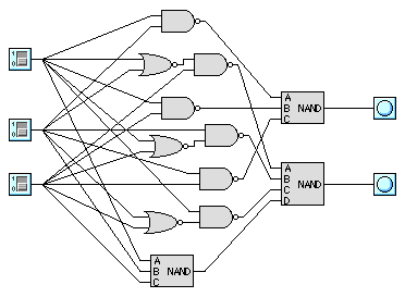
What does this circuit do?
It is a full adder.
-
Using truth tables and/or boolean logic, prove your statement about what
the circuit does.
First, we'll consider the top output. If we name the inputs on the left A, B, and C, then the top output is ~(~(AB)~(AC)~(BC)). By DeMorgan's Law, this is equivalent to AB+AC+AB. This is the "carry-out" output of the full adder.
The bottom output is ~(~(~(A+B)C)~(~(A+C)B)~(~(B+C)A)~(ABC)). By DeMorgan's Law, this is equivalent to ~(A+B)C+~(A+C)B+~(B+C)A+ABC. Again by DeMorgan's Law, this is equivalent to ~A~BC+~AB~C+A~B~C+ABC. In other words, the second output is true if only one or all three inputs is true. This is the "sum" output of the full adder.
-
How many transistors (minimum) would be required to implement this circuit?
28, one for each input for each gate.
See Fig. 3-29(a) of Tanenbaum.
-
Explain its function.
It is used to disconnect a logic circuit from a line. This allows other logic circuits to use the same line.
-
How many inputs does it have? How many outputs?
It has two inputs, and one output. One input is called Data In, the other Control. The output is called Data Out.
-
Give a table showing all outputs for all combinations of inputs.
Data In   Control   Data Out
   0         0        none
   0         1          0
   1         0        none
   1         1          1
The new chip, as designed, has 16 address pins, 8 bi-directional data pins, three status outputs (MREQ, R/~W, DRDY), two control inputs (RESET, MACK) and pins for clock input, Vcc, and Gnd. MREQ is asserted when the address is stable and a memory read or write is needed. R/~W is asserted if a memory read is requested, and negated if a write is requested. DRDY is asserted during a memory write when the address, data, and other status outputs are stable and during a memory read when the CPU is ready to receive data. RESET is used to put the chip into a pre-defined start state, and MACK is used to indicate that the data are available for reading (or that the write is complete) and is held asserted until DRDY is negated.
The team leader presented this design and was clearly proud of the team's work; so much functionality had been squeezed into 32 pins.
-
Draw a timing diagram that illustrates the relative timings
and dependencies for the address, data, and MREQ, R/~W, DRDY,
and MACK pins for a memory read.
____ ____________________ ______ Addr ____X____________________X______ ____________________ R/~W ____/ \______ ___________________ MREQ _____/ \______ ______________ DRDY ______/ \__________ ______________ ________ ________ Data ______________X________X________ _______ MACK _______________/ \________ -
Would you recommend a synchronous or asynchronous bus for
communication between the CPU and the memory and other devices?
Explain your answer.
Actually, either would work. There are enough hand-shaking signals to support an asynchronous bus, and for this application this should not be too difficult to implement.
-
What functions commonly found on a general purpose chip are missing?
Most notably, there are no pins dealing with I/O interrupts nor for bus arbitration.
-
You're aware that the customer doesn't have tooling to manufacture
boards for chips having more than
32 pins. How might the team add functionality requiring 8 additional
pins without increasing the pin count? Assume that it is acceptable
to add a few inexpensive chips to the board used by the CPU.
The easiest approach might be to combine the 8 data pins with the 8 low-order address pins. The 8 low-order address pins could be latched by 8 flip-flops clocked on MREQ, and the same pins could be driven by a bi-directional non-inverting buffer controlled by DRDY, R/~W, and MACK.